


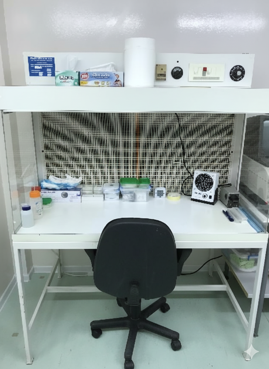
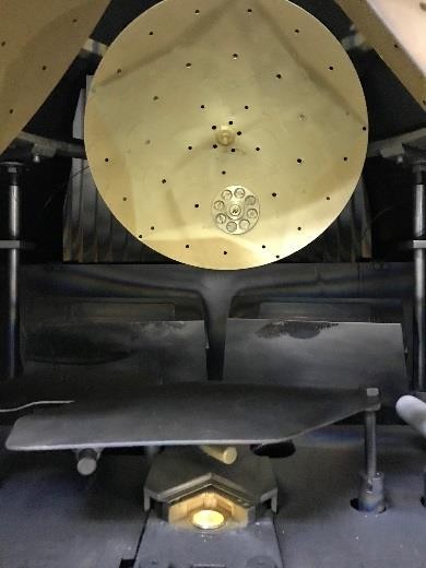
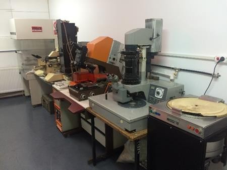
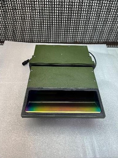
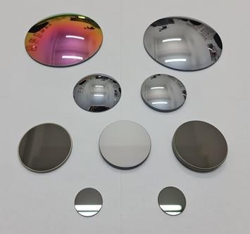
PVD – CVD COATINGS
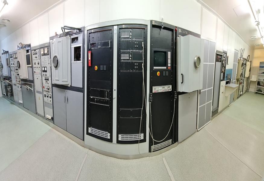
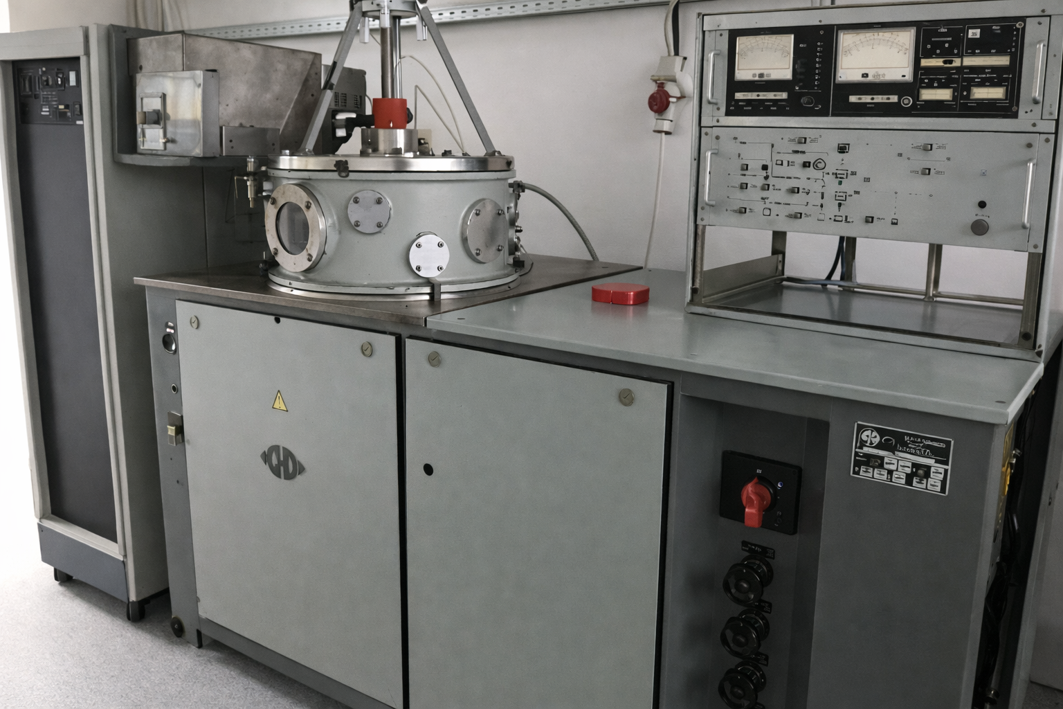
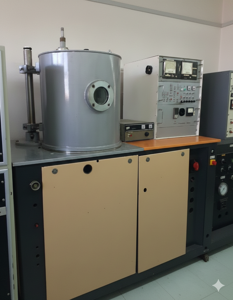
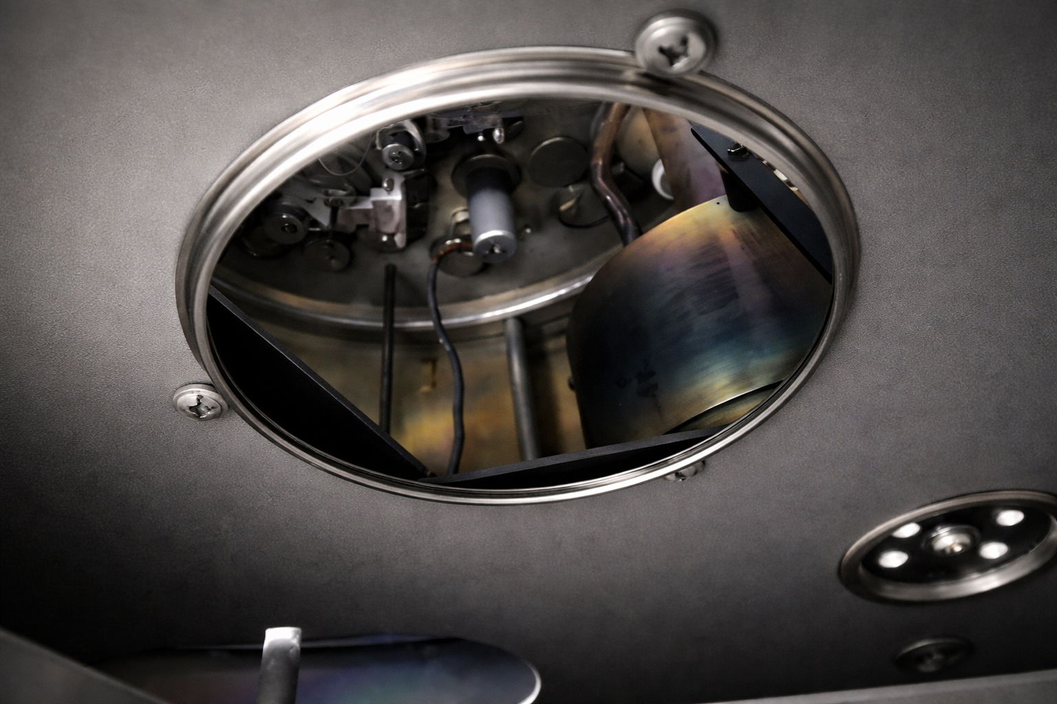
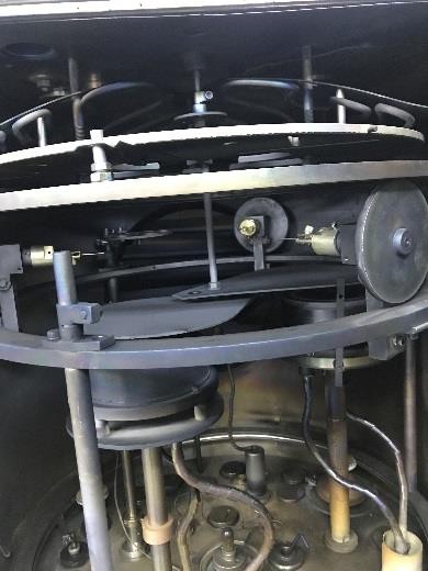
A714 Leybold, VU-2M-Optics, BAK-550-Balzers, BAK-600-Balzers - Thermal, E-gun, physical and optical monitoring
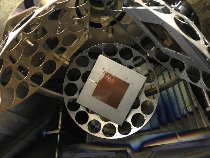
VU-2M-S, BAS-450-PM Balzers, Z-550-S Leybold, MAGNETRON – DC, RF and HiPIMS sputtering
VU-2M-S, BAS-450-PM Balzers, Z-550-S Leybold, MAGNETRON – DC, RF and HiPIMS sputtering
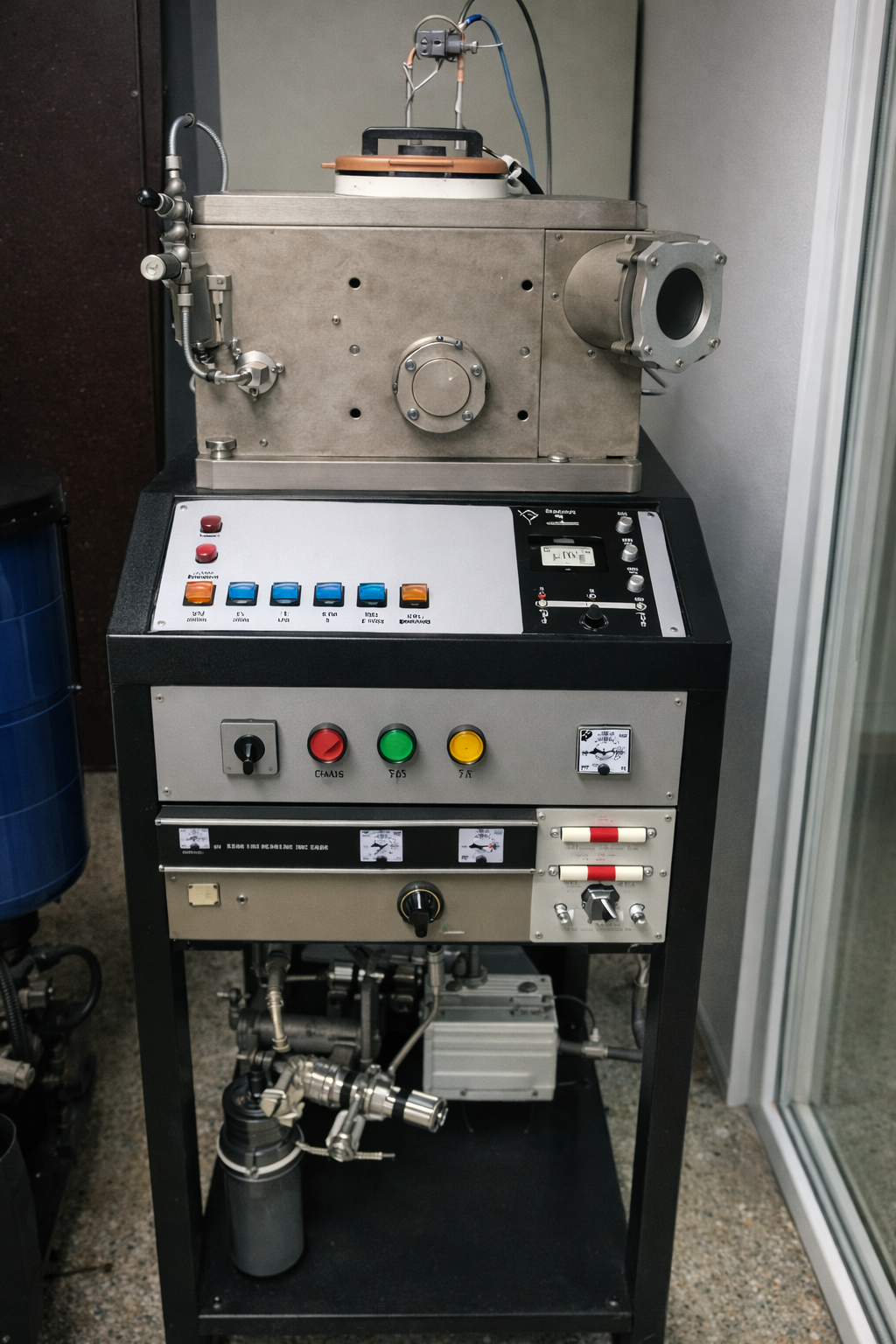
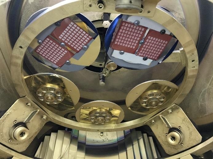
PECVD – DLC (Diamond-Like Carbon) - optical IR coatings RIE-
MGM and PECVD-MGM – Plasma Etching and Coatings
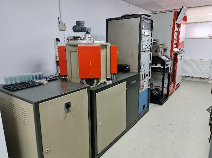
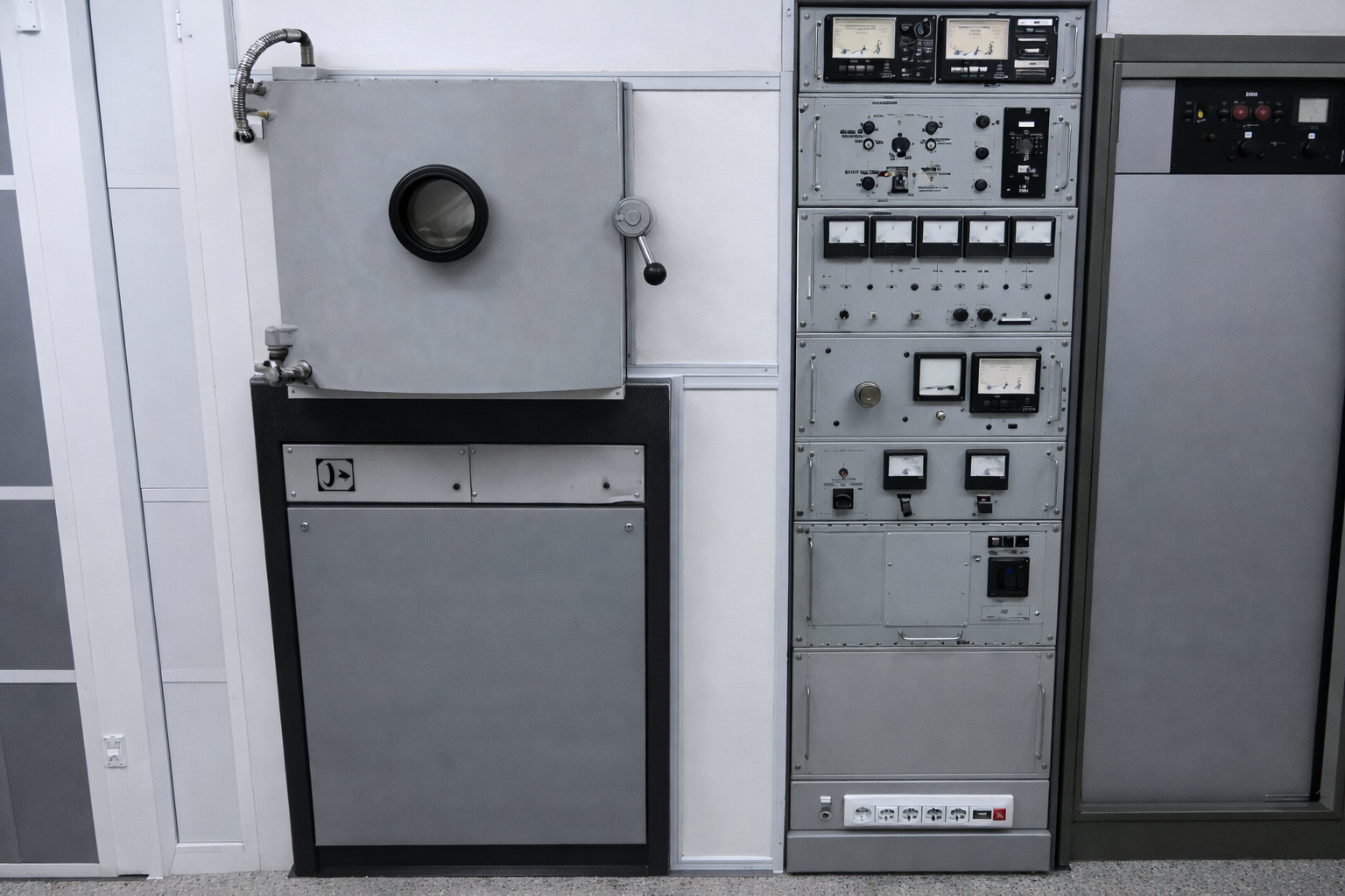
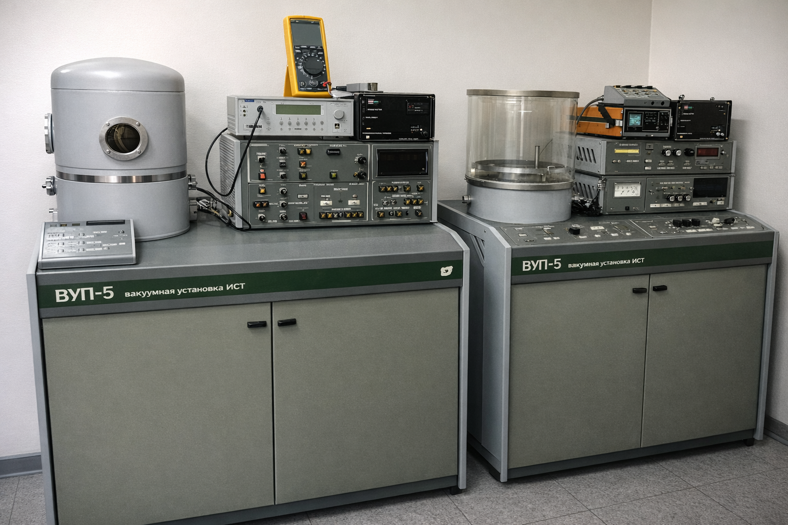
D-MGM – DC sputtering - metallic coatings on industrial diamonds VUP-5 –
Thermal, DC and RF sputtering
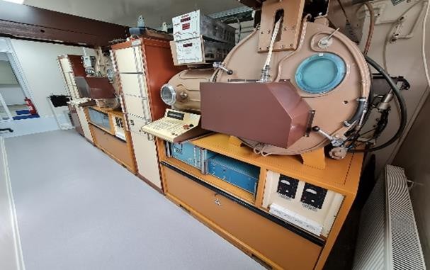
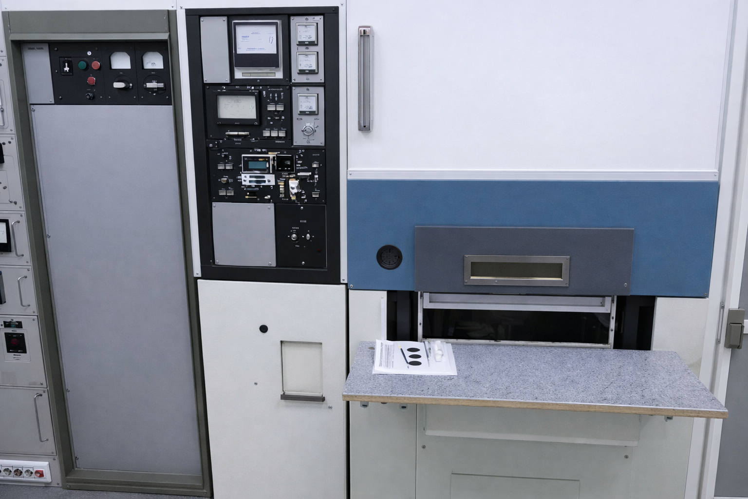
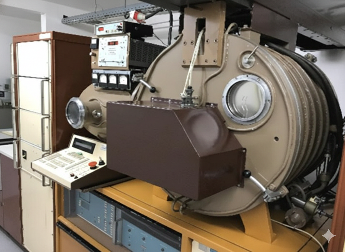
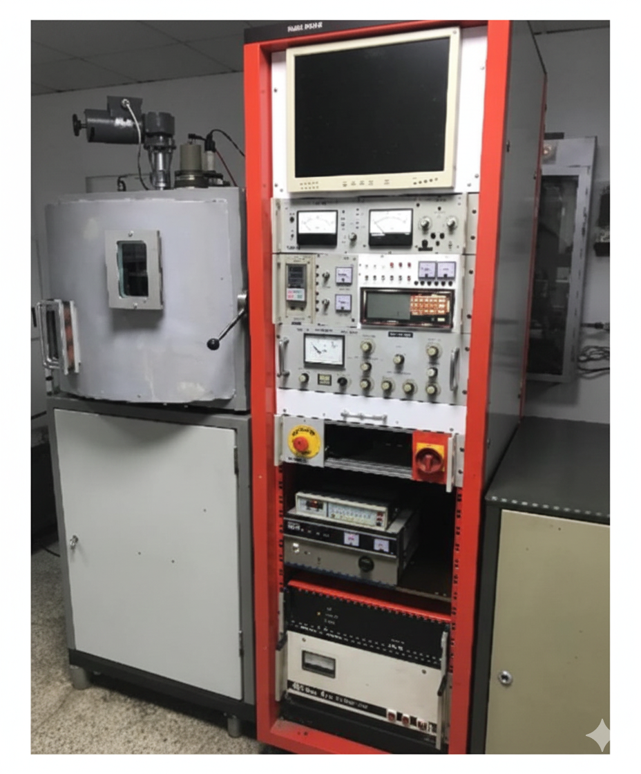
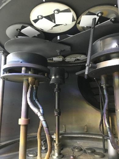
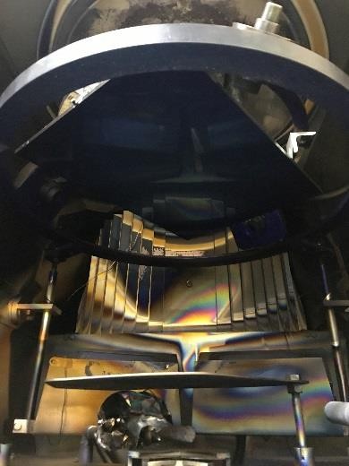
VU-1BS – Cathodic-Arc and BIAS - hard, low friction and decorative coating
MGM and PECVD-MGM – Plasma Etching and Coatings
D-MGM – DC sputtering - metallic coatings on industrial diamonds VUP-5 –
Thermal, DC and RF sputtering
VU-1BS – Cathodic-Arc and BIAS - hard, low friction and decorative coating
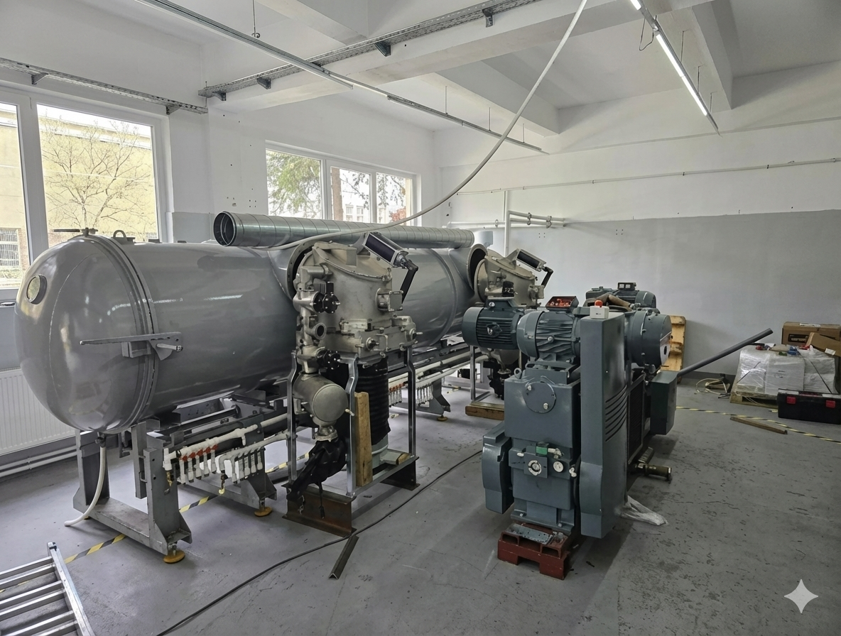
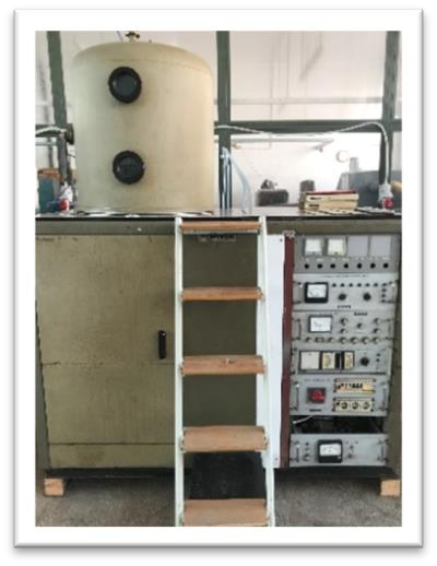
MAS-10-1,2x6m and DM-1200 2 doors – In implementation stage - Cathodic-Arc and Thermal – hard and decorative coatings
MAGNETRON – DC sputtering – roll-to-roll system
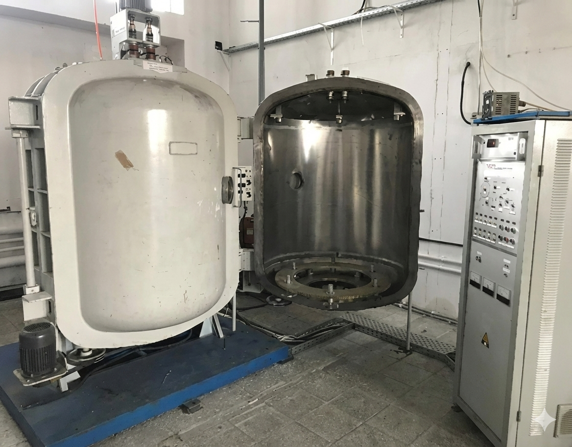
B-55 - Cathodic-Arc and DC sputtering – metallic coatings
UVO – 6/8 2” cathodes - DC- F-HiPIMS sputtering – HEA coatings
BA-710 Balzers – Cathodic-Arc – antimicrobial and photocatalytic coatings
MAGNETRON – DC sputtering – roll-to-roll system
B-55 - Cathodic-Arc and DC sputtering – metallic coatings
UVO – 6/8 2” cathodes - DC- F-HiPIMS sputtering – HEA coatings
BA-710 Balzers – Cathodic-Arc – antimicrobial and photocatalytic coatings
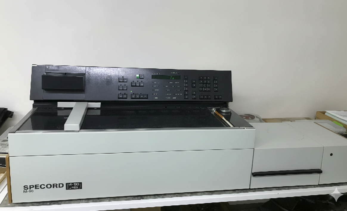
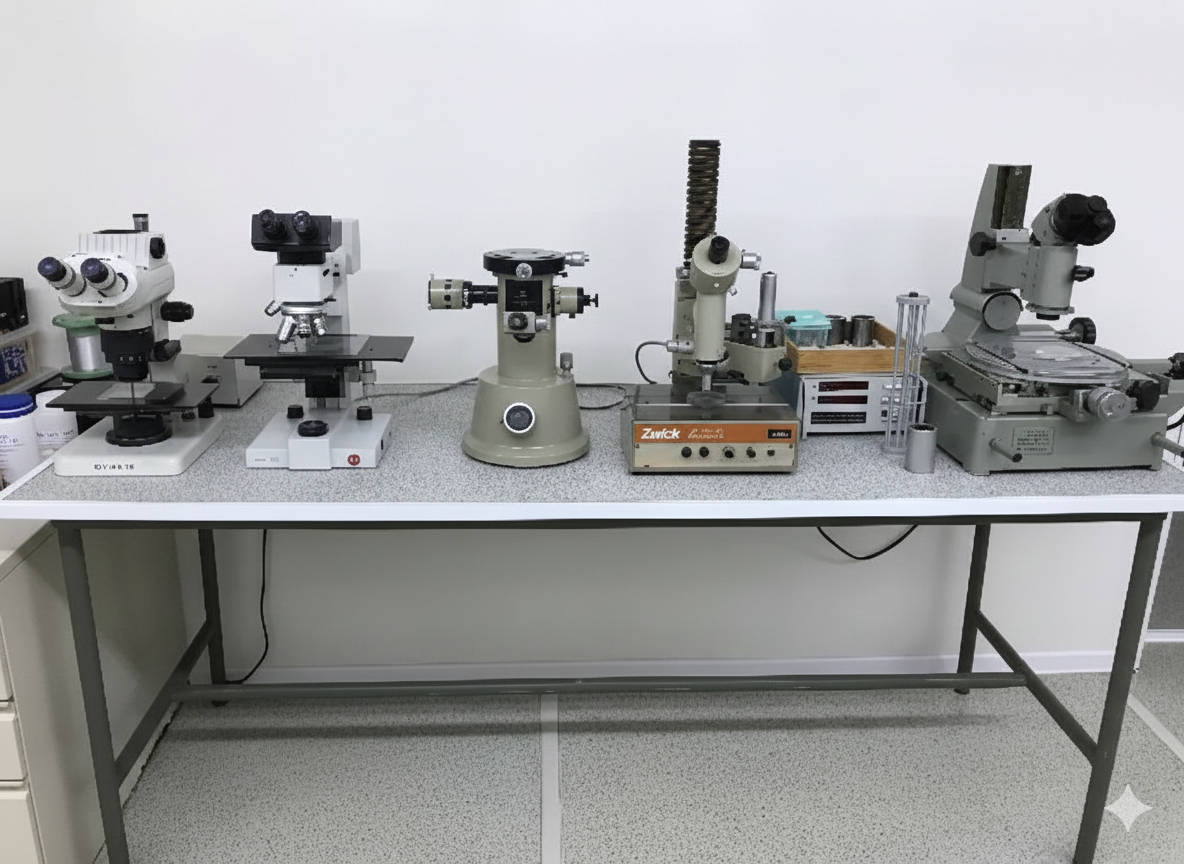
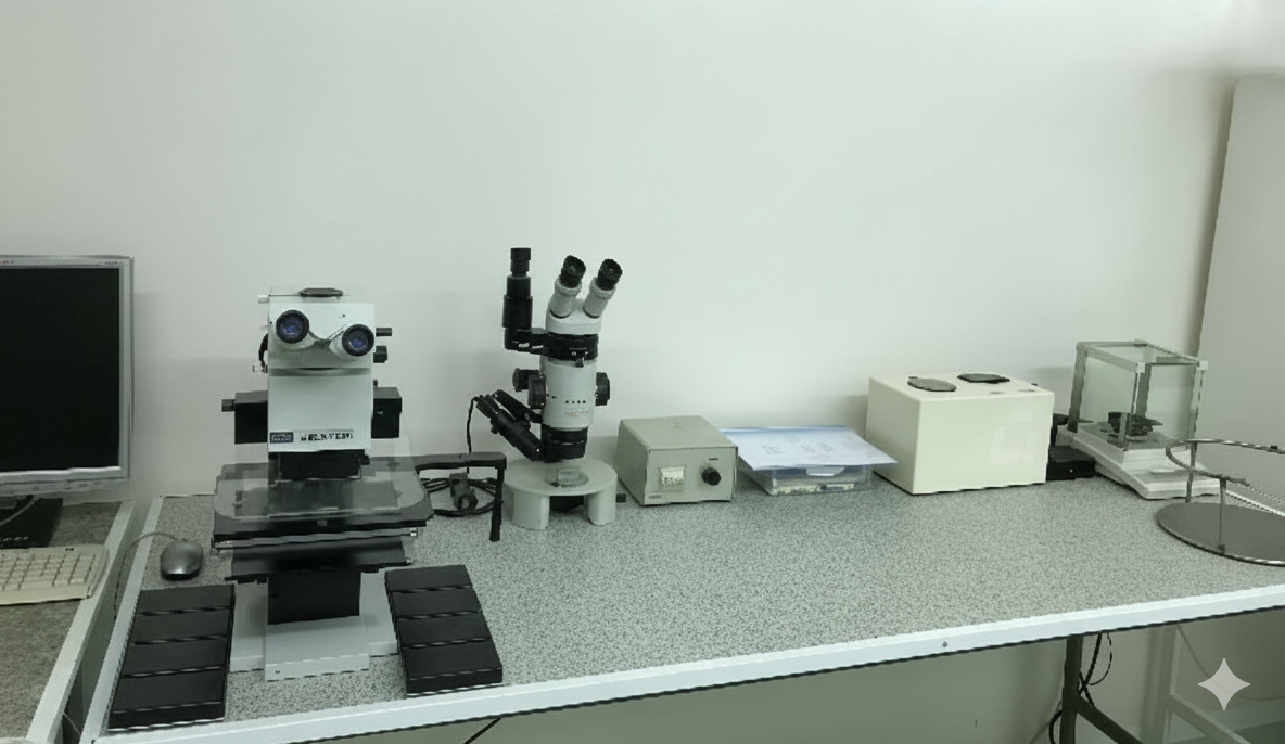
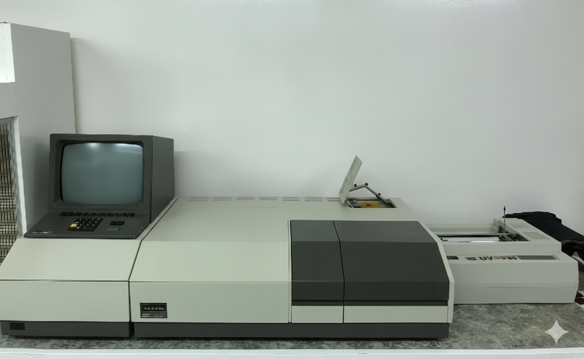
COATINGS CHARACTERIZATION
DLC on Si and Ge optical component for thermal imaging cameras and night vision systems
ITO on imaging systems and aircraft window
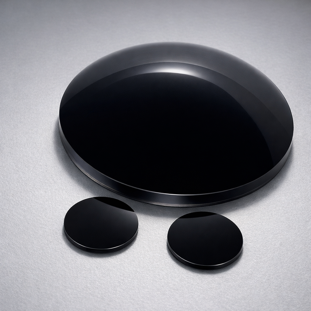
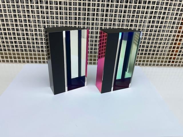
TiAlN for laser power meters sensors
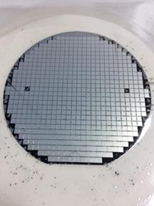
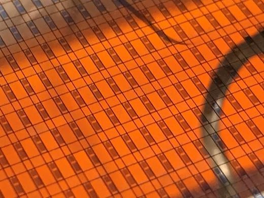
H-free DLC, Al, Ti-Ni-Ag/Au on Si wafers - microelectronics structures Au on polyamide osteoporosis sensors
ITO on imaging systems and aircraft window
TiAlN for laser power meters sensors
H-free DLC, Al, Ti-Ni-Ag/Au on Si wafers - microelectronics structures Au on polyamide osteoporosis sensors
COATINGS SERVICES
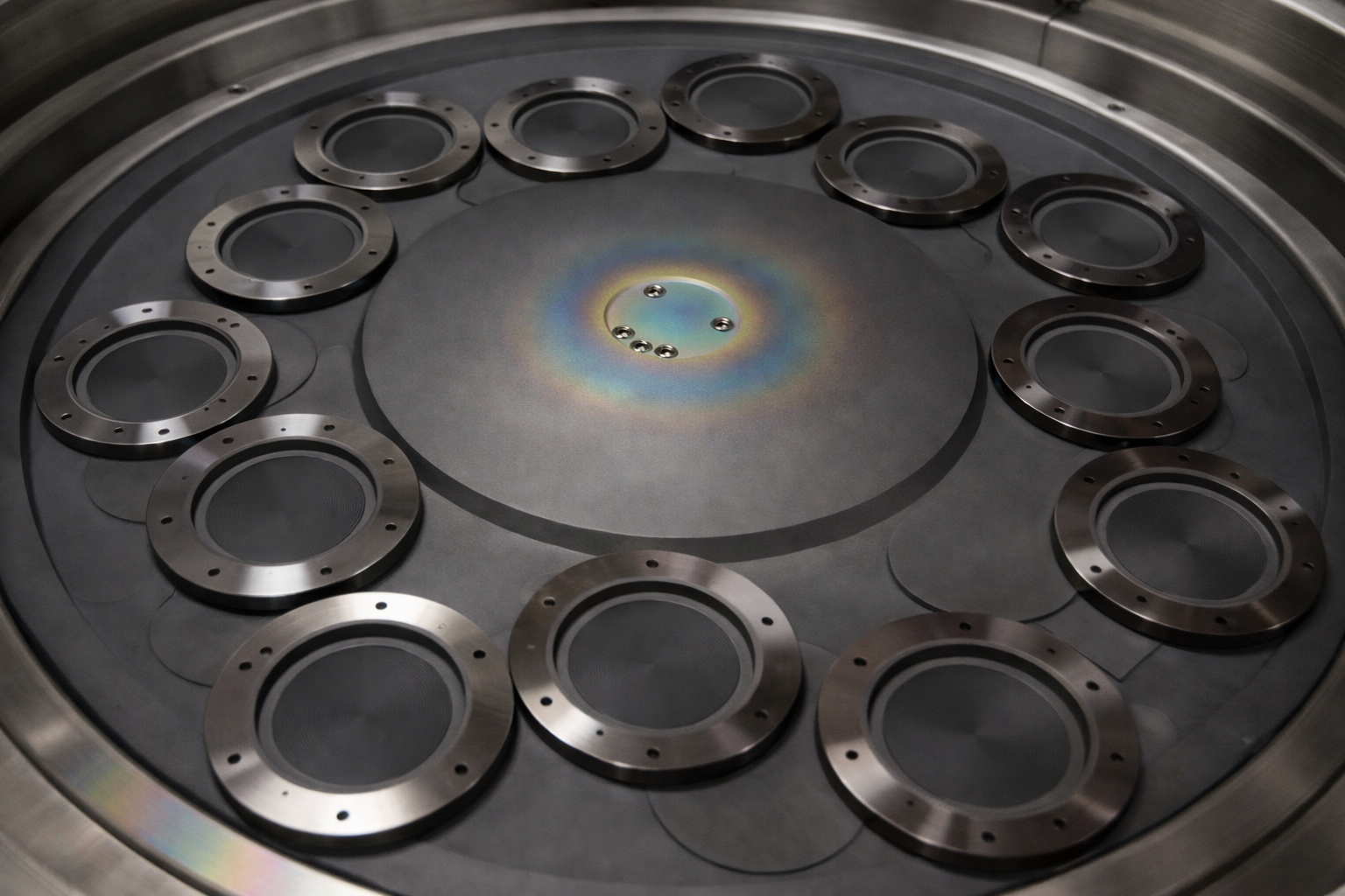
DLC on Si and Ge optical component for thermal imaging cameras and night vision systems
ITO on imaging systems and aircraft window
TiAlN for laser power meters sensors
H-free DLC, Al, Ti-Ni-Ag/Au on Si wafers - microelectronics structures Au on polyamide osteoporosis sensors
ITO on imaging systems and aircraft window
TiAlN for laser power meters sensors
H-free DLC, Al, Ti-Ni-Ag/Au on Si wafers - microelectronics structures Au on polyamide osteoporosis sensors
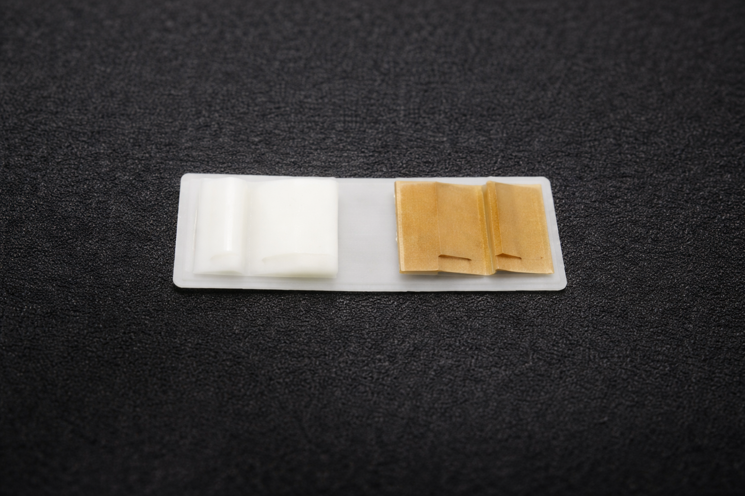
TiCN on pistons, DLC on bearings axles, Gd on Al plate (X-ray shielding), Pt on alumina (sensors),
Au on alumina (sensors) and on precision quartz sensors
Cr-Ni-Au/Ag on Si and Kapton supports (sensors)
Au on alumina (sensors) and on precision quartz sensors
Cr-Ni-Au/Ag on Si and Kapton supports (sensors)
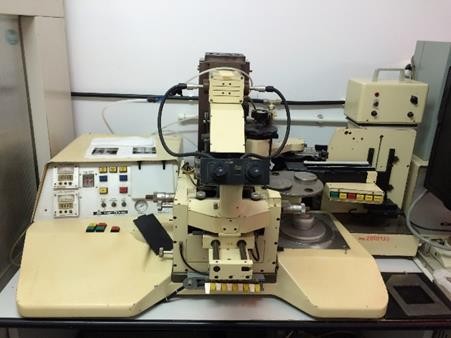
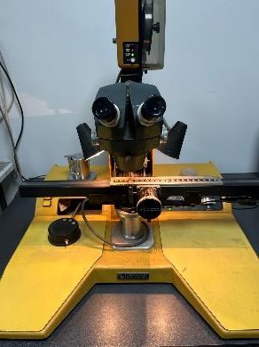
LITHOGRAPHY FACILITIES
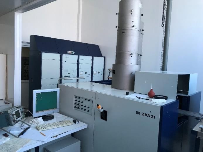
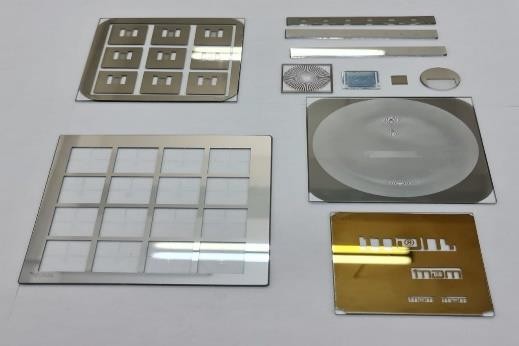
Electron Beam Lithography System
ZBA 21 CARL ZEISS JENA
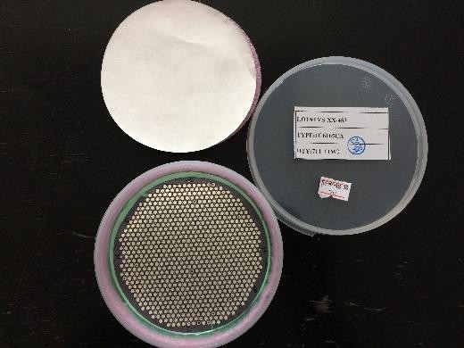
Full line for etalon and work masks up to 7x7 inches or diam. 6 inches resolution up to 0,2 microns
Reticles, Computer Generated Holograms, Fresnel Lenses, Diffractive Optical Elements, gas, liquid and
neurological sensors, high precision quartz sensors, metallic graphics
ZBA 21 CARL ZEISS JENA
Full line for etalon and work masks up to 7x7 inches or diam. 6 inches resolution up to 0,2 microns
Reticles, Computer Generated Holograms, Fresnel Lenses, Diffractive Optical Elements, gas, liquid and
neurological sensors, high precision quartz sensors, metallic graphics
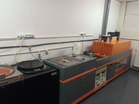
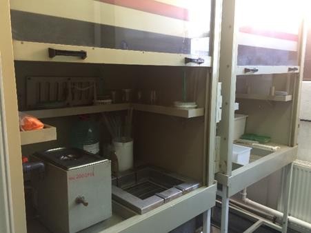
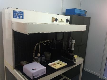
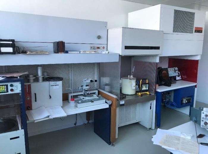
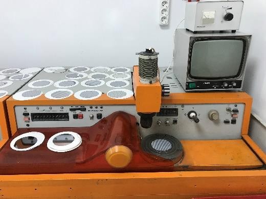
The company has full photolithographic line
Ovens, centrifuges, masks cleaning, photoresist spin-coating and IR treatment
Single side, double side and with proximity alignment and UV exposure
Ultrasonic cleaning, wet chemical etching, control
Ovens, centrifuges, masks cleaning, photoresist spin-coating and IR treatment
Single side, double side and with proximity alignment and UV exposure
Ultrasonic cleaning, wet chemical etching, control
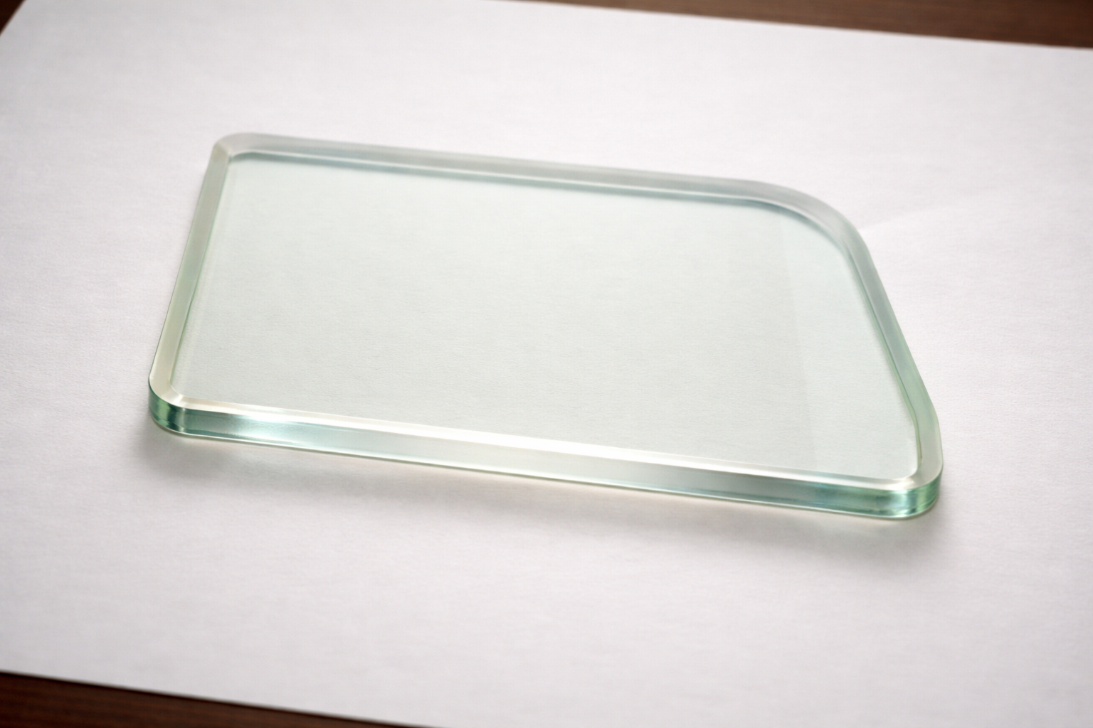
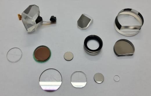
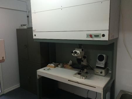
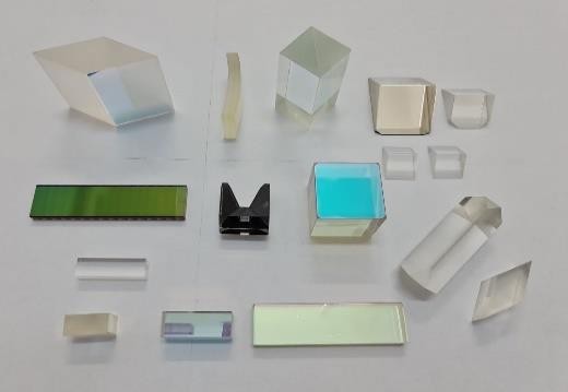
OPTICAL FACILITIES
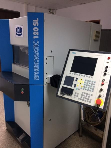
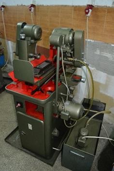
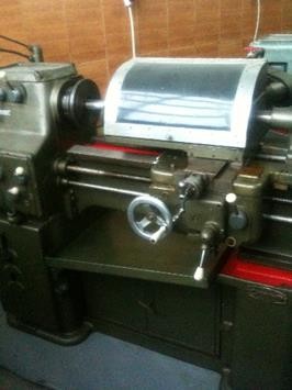
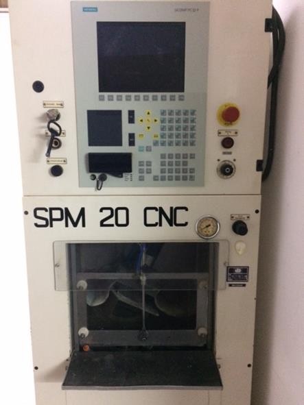
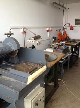
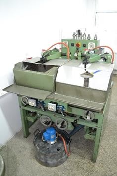
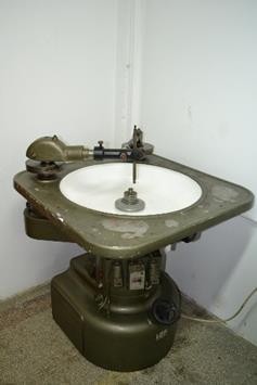
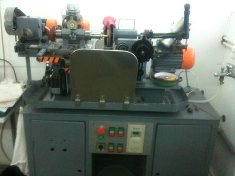
The company has full line for optical manufacturing
Cutting, CNC grinding and polishing, prism and cube grinding, lens and plano grinding and polishing, centering.
Cutting, CNC grinding and polishing, prism and cube grinding, lens and plano grinding and polishing, centering.
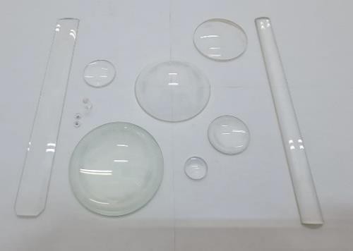
The company has full line for optical manufacturing
Cutting, CNC grinding and polishing, prism and cube grinding, lens and plano grinding and polishing, centering.
Cutting, CNC grinding and polishing, prism and cube grinding, lens and plano grinding and polishing, centering.
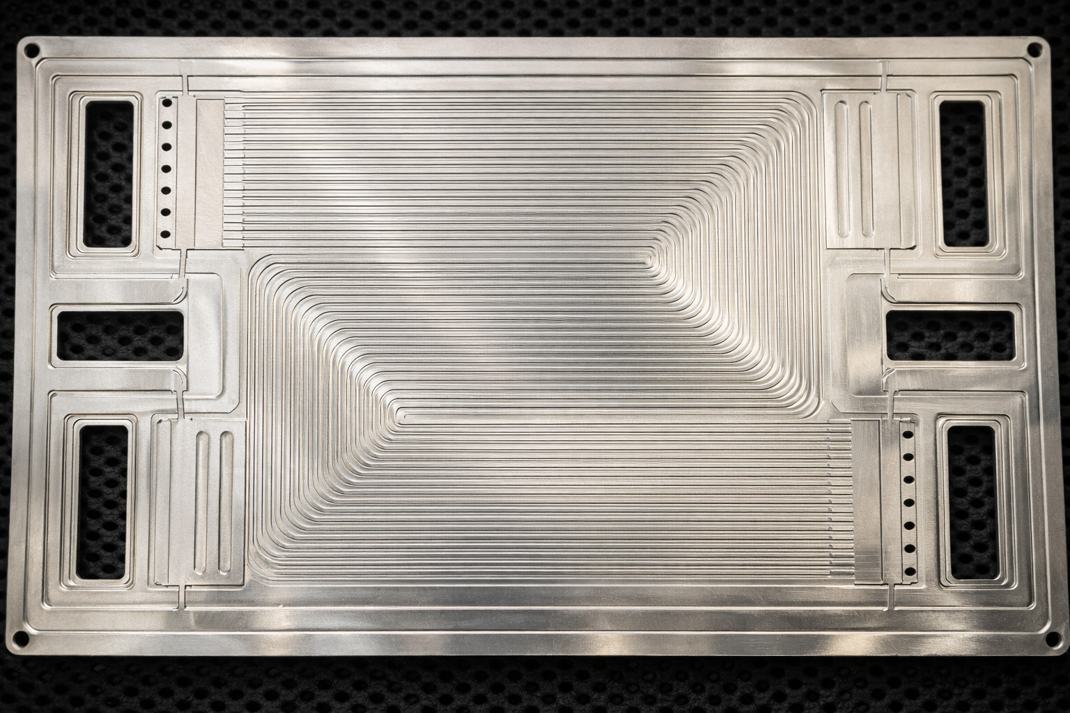
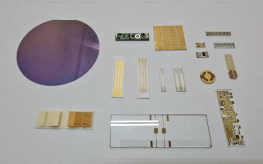
MICROELECTRONICS APPLICATION
Ultrasonic wedge bonding
Processing Si wafers with power diode structures - remove Al coating, Ag/Au coating, lithography/lift-off, cutting of structures
Neurological sensors – coating Au on Si and Kapton foil, lithography/lift-off, cutting, microfire welding
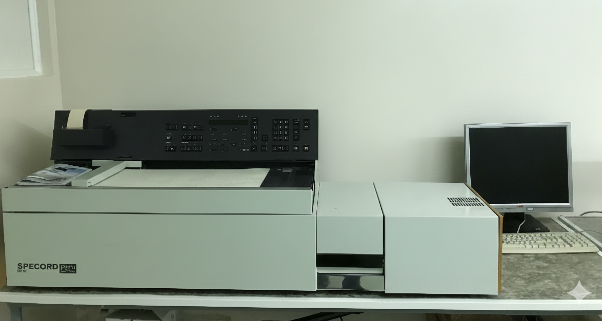
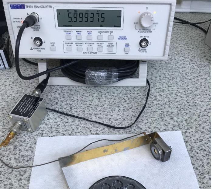
Frequently controlled coating for precision quartz crystals
Helium leak mass spectrometer test
Processing Si wafers with power diode structures - remove Al coating, Ag/Au coating, lithography/lift-off, cutting of structures
Neurological sensors – coating Au on Si and Kapton foil, lithography/lift-off, cutting, microfire welding
Frequently controlled coating for precision quartz crystals
Helium leak mass spectrometer test